ATmega AVR Code Example
Apr 16, 2016 By Islam Essam
In this article I will explain some basic fundamentals on the ATmega architecture and deliver a simple example built in AVR Studio that will summarize the material. This tutorial is made for entry level developers with little to no experience with the 'C' programming language.
Tools
- AVR Atmel studio / AVR studio Examples will be in "AVR Studio 4.0", but you can use any other version. For a quick reference, you can take a look the quick start guide: Getting-started-Atmel_studio
- AVR kit to run your code (use ATmega 8/16/32). You can pick-up a starter kit or a home made one with a programmer. Check out ATmega8 resources on the Atmel-Atmega_page
- Proteus Virtual simulator
Table of Contents
- AVR Microcontroller Overview
- Peripheral Basics (I/O)
- pseudo code
- Simple Application
AVR Microcontroller Overview
The Microcontroller is a collection of modules gathered on single chip. The microcontroller contains a CPU (central processing units) that interacts with its peripherals. The ALU (arithmetic logic unit) performs Instructions ( Add, Sub, AND, OR, Xor, ...etc)
 This includes:
Memory
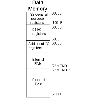
- Program Memory Holds instructions that "tells the microcontroller what to do". AVR uses FLASH memory for the program memory. FLASH is a type of memory that can be written to multiple times, often millions, without beign corrupted. It retains its values over power cycles. This is different than RAM in which the data is lost after a power cycle. ATmega8 -> "8" refers to the size of Flash = 8 Kb , (4K * 16-bit ) == 4K Instructions "Max Program size".
- Data Memory Holds data used by the program (i.e Variables, tables , pointers, structures, constants, Logs ...etc). This is amount is limited to only 1024 bytes in the ATmega8 family.
- RAM Used to hold dynamic variables ( Global, static, heap, stack variables) i.e all what the program need to change as it run. The type of RAM availaible is called static RAM (SRAM). This means that the data is kept unchanged even without the clock present which typically happens on microcontrollers when it is sleeping (clock is OFF). Contrast this with dynamic RAM which relies on a constant clock signal that is typically found in desktop machines.
- E2PROM Used to hold user-defined variables with scope beyond to the program RUN cycle.
- Special Function Registers These registers are special since they directly interace with the specific ATmega hardware. There are 96 Registers (I/O) in total on the ATmega8.
Clock
In order for the microcontroller to execute code from program memory, it needs a clock to synchronize the internal transistors to move data between registers.
Peripheral Basics (I/O)
How do we interact with the outside world? You interact via the microcontroller pins whether its reading a value, toggeling an LED ON, or writing to a display. There are two types of signals:
- Analog Variable voltage levels. Examples would be audio or motor voltage feedback.
-
Digital Two distinct levels which typicall correlate to a digital
1or0value. Examples include a clock source or a switch.
Here is a picture of the ATmega8 pin diagram.
 There are many hardware pins with some being digital, analog, or mixed functionality. Each pin usually could be used to do function at a time, but pin could serve for multiple use, different applications
WHO do you think should tell Those pins What to do ?!
There are many hardware pins with some being digital, analog, or mixed functionality. Each pin usually could be used to do function at a time, but pin could serve for multiple use, different applications
WHO do you think should tell Those pins What to do ?!
- Of course It's YOU the one who develop the applications
- but THROUGH the MASTER mind of the System the CPU "Microprocessor" YOU tell the CPU what to do by Instructing it, to do so you need to know how it interact with the peripherals ... After we almost figured out what is in there, it is time to know how all that collaborate together Let's agree on something first, What is a microprocessor !? we agree that it is a !!! DIGITAL !!! Device that perform Operations (i.e instructions) operations on WHAT!?? -> On !!! DATA !!! what type of Data?? -> yeah, !!! DIGITAL !!! Data Then now what we use microprocessor for:
- Read data ( from memory / Devices / ...etc)
- Operate on Data ( Inside the CPU , ALU)
- write data ( To Memory / Devices / Screens ...etc)
now we see that it is all about DATA ... and " READ , Write " it then operate when needed
How the processor knows WHERE to Read data from ??
here we all know that no package leaves the office without the "Destination Address", or it will be lost
here is the same, every Peripheral/Device within our system (i.e inside microcontroller itself) should have Address
that way we can use that address to READ from or Write to
!!! Mission Accomplished !!!
The CPU (i.e Microprocessor), Only Have 2 things (Address bus , Data bus) to Interact with outside world
Only RAM is fully compatible with that, It has (Address bus, Data bus) , because its Memory (i.e Addressed Locations)... !!! Perfect !!!
UNfortunately ADC , and Digital Devices "I/O interface" are pure electronics with no Addresses !!!
WHAT about those Devices Those Don't have Address and Data bus by nature !?
well, Let's Give them an Address and Data Bus, O.o !!! How is that !!!??
Those Devices need a Translator between them and the microprocessor to be able to operate together
That's why Each peripheral provide a SET of Control/Data registers for the CPU to understand
check the following diagram
 here we understand that, the Peripheral being Control by the CPU through it's control(Configuration) registers
and read/write Data through the data registers
That's how CPU interact with any peripheral, by Giving an address to each Register and then talk to it as if it was a Memory.
As we discussed "Memory RAM" already addressed, how about the peripheral??
Actually every part occupy a space in the Address space that the Address bus can span
check the next figure
here we understand that, the Peripheral being Control by the CPU through it's control(Configuration) registers
and read/write Data through the data registers
That's how CPU interact with any peripheral, by Giving an address to each Register and then talk to it as if it was a Memory.
As we discussed "Memory RAM" already addressed, how about the peripheral??
Actually every part occupy a space in the Address space that the Address bus can span
check the next figure
 Now we should conclude everything in simple points:
 - CPU Deal with memory
- Every thing else should operate the way a processor can understand
- Registers are Memories, and it act as the interface between the CPU and any operation it need to perform on other hardware
- Registers
- System Registers < to control / monitor system/microcontroller/ peripherals : called SFR , IO , ADC , Status Reg
-
General purpose Registers < GPR>: for general use by programmer as a fast memory R0-R31 (Assembly programmers scope)
SFR exmples ATmega8
 ##nature of the Peripheral (basic Peripheral I/O )##
After we covered how the processor interface ( Control / Exchange data R/W) with any peripheral
Its important to mention that each peripheral has different functionality and so different configuration and also different Data in both meaning and format
In this part of our series we'll discuss the I/O peripheral, usually called GPIO general purpose Input Output
GPIO is Responsible for any interface with the outside world including (Data exchange from parallel port for example, serial, Motor
control, sensor signal)
So it is a must to master GPIO operation in order to proceed with the Embedded world.
GPIO pins are the arranged in the Given PORTs of the Microcontroller
##nature of the Peripheral (basic Peripheral I/O )##
After we covered how the processor interface ( Control / Exchange data R/W) with any peripheral
Its important to mention that each peripheral has different functionality and so different configuration and also different Data in both meaning and format
In this part of our series we'll discuss the I/O peripheral, usually called GPIO general purpose Input Output
GPIO is Responsible for any interface with the outside world including (Data exchange from parallel port for example, serial, Motor
control, sensor signal)
So it is a must to master GPIO operation in order to proceed with the Embedded world.
GPIO pins are the arranged in the Given PORTs of the Microcontroller - GPIO
- Digital GPIO
- All PORTs ARE Digital GPIO enabled
- All pins could operate INPUT OR OUTPUT ( configurable )
- Analog GPIO
- Only selected pins can operate as Analog pins to work as input for ADC ( to be covered later in the ADC part of the series ) In this part of the series we will Cover Digital GPIO In ATmega family To control the GPIO module, you've been given Set of Registers to fo So
DDR -> (DDRA , DDRB , DDRC , DDRD , ...etc for larger IC's)
PORT -> (PORTA , PORTB , PORTC , PORTD , ...etc )
PIN -> (PINA , PINB , PINC , PIND , ...etc) |Address|NAME|bit7|bit6|bit5|bit4|bit3|bit2|bit1|bit0| |:---------:|:-------|:-------|:-------|:-------|:-------|:-------|:-------|:-------|:-------| |0x18 (0x38)| PORTB | PORTB7 | PORTB6 | PORTB5 | PORTB4 | PORTB3 | PORTB2 | PORTB1 | PORTB0 | |0x17 (0x37)| DDRB | DDB7 | DDB6 | DDB5 | DDB4 | DDB3 | DDB2 | DDB1 | DDB0 | |0x16 (0x36)| PINB | PINB7 | PINB6 | PINB5 | PINB4 | PINB3 | PINB2 | PINB1 | PINB0 | |Hardware Pin| -> |Pin7|Pin6|Pin5|Pin4|Pin5|Pin4|Pin3|Pin0| |############|#######|########|########|########|########|########|########|########|########| AS we see Every PORT ( 8 hardware Pins ), has 3 control registers after its name (PORT , DDR , PIN) Each is 8-bit Register, where every "bit 0-7" is mapped to the corresponding "Pin 0-7"
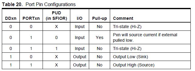
- DDR Data Direction Register (DDRA , DDRB , DDRC , DDRD ,...) this Register is used to Configure Pins to in a given port to be INPUT or OUTPUT setting bit7 in DDRB (i.e DDRB bit7 = 0b1 ) -> PortB pin7 is now "OUTPUT" Clearing bit6 in DDRB (i.e DDRB bit6 = 0b0 ) -> PortB pin6 is now "INPUT"
- PORT (PORTA , PORTB , PORTC , PORTD ,..) this Register is named after the PORT itself when we Configure PIN as OUTPUT -> we Set the value of this pin in the PORT REG After we have configured PortB pin7 as output , we now control the output Setting bit7 in PORTB (i.e PORTB bit7 = 0b1 ) -> PortB pin7 now Sourcing Logic high -> pin7 volt = VDD (~3-5 v) LOGIC HIGH = 1
- PIN (PINA , PINB , PINC , PIND , ...) this Register is named after the PINs when we configure PIN as INPUT -> we READ the value of this pin from the PIN REG After we have configured PortB pin6 as Input , we now ready to read the INPUT value Reading PINB bit6 --> now we know if bit6 = 0b0 -> input low (~0v) , if bit6 = 0b1 -> input high (~3-5 v)
-
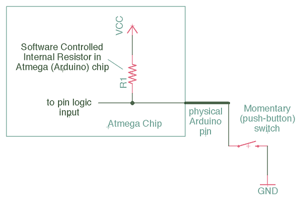
pull-up
this was the simple configuration of a Port pins to be output / input
In case the Port pins are Configured as input, the controller act as a SINK for the derived current
and if the current exceeded a calculated limit this could harm the chip
For that Reason they have designed the Sink current as a Reference of the VDD supply with the so called "Rpu"
Rpu Limits the Sink current and make the buss High until any other device pulled it Down so the input become Low.
this setup is fine with application those in a need to sense input level change due to external driving.
Check the figure below
 if this setup not fitting your setup, as you may need to not use the pull-up resistance and use the Tri-state
that way you will be able to externally drive the bus High , and , Low as needed (take care of the Current you pass ;) )
Oh!!
one more Thing "Pull-up" feature should be enabled First of All on the Microcontroller
System wide "pull-up" MUST be enabled First
PUD bit in SFIOR Register, check the following image
if this setup not fitting your setup, as you may need to not use the pull-up resistance and use the Tri-state
that way you will be able to externally drive the bus High , and , Low as needed (take care of the Current you pass ;) )
Oh!!
one more Thing "Pull-up" feature should be enabled First of All on the Microcontroller
System wide "pull-up" MUST be enabled First
PUD bit in SFIOR Register, check the following image
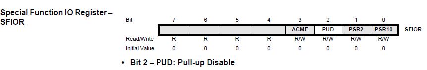 to enable PUD bit-2 in the SFIOR , its enabled by default "PUD = 0b0"
if "PUD = 0b1" , the Pull-up is Disabled System wide
To activate the Pull-up option you need to configure the Input pin with extra configuration
to enable PUD bit-2 in the SFIOR , its enabled by default "PUD = 0b0"
if "PUD = 0b1" , the Pull-up is Disabled System wide
To activate the Pull-up option you need to configure the Input pin with extra configuration - Configure the pin as INPUT , Portb Pin6 , now we could use PINB register to monitor its value
- Set the Corresponding bit in the PORT register in order to Activate the Pull-up
Setting bit6 in PORTB ( i.e PORTB bit6 = 0b1 )
NOW "PortB Pin6 is INPUT & Pulled-up"
The following figure contain a table that summarize all combinations needed for Pin to be Configured
- INTERRUPT " EXTERNAL INTERRUPT " T his Is a mode of Operations for PINs IT is Clarified in the INTERRUPT section of Series part III under_construction link ##pseudo code of how to make it work the propper way ##
- DIGITAL
- OUTPUT Let's Select PortC Pin3 to be Output and Write 0b1
/* configure the Pin as OUTPUT write 0b1 to the bit3 in DDRC REG */
DDRC |= 1 << 3 // this way we only change bit3 without affecting any other PINs on PortC
/* Drive the Pin HIGH ( put VDD on the hardware PIN ) */
PORTC |= 1 << 3 // this to only update Pin3 output voltage only
- INPUT
- INPUT_FLOATING Let's Select PortB pin5 to be INPUT
/* configure the Pin as INPUT write 0b0 to the bit3 in DDRB REG */
DDRB &= (~(1 << 5)) // this way we only CLEAR bit5 without affecting any other PINs on PortB
/* Read the value from Pin5 in PINB REG */
__READ_VAR = PINB & (1 << 5) __ // his to only Read Pin5 INPUT Level from PINB
IF (READ_VAR ) { Print: __INPUT LEVEL HIGH : LOGIC 1 __} // THE INPUT IS HIGH "Logic 1 "
else {Print: __INPUT LEVEL LOW : LOGIC 0 __} // the input is Low " LOGIC 0 "
- INPUT_PULLED_UP Let's Select PortB pin3 to be INPUT
/* Enable the PUD pull-up feature system wide this to be ENABLED only once per application PUD bit2 in SFIOR = 0 */
SFIOR &= ( ~(1 << PUD)) // this enables the PULL_UP system wide
/* configure the Pin as INPUT write 0b0 to the bit3 in DDRB REG */
DDRB &= (~(1 << 3)) // this way we only CLEAR bit3 without affecting any other PINs on PortB
/* Let's Enable PULL_UP for Pin3 PORTB PORTB bit3 = 0b1*/
PORTB |= 1 << 3 // Set PORTB bit3 to enable PULL_UP on PORTB Pin3
/* Read the value from Pin3 in PINB REG */
__READ_VAR = PINB & (1 << 3) __ // his to only Read Pin3 INPUT Level from PINB
IF (READ_VAR ) { Print: __INPUT LEVEL HIGH : LOGIC 1 __} // THE INPUT IS HIGH "Logic 1 "
else {Print: __INPUT LEVEL LOW : LOGIC 0 __} // the input is Low " LOGIC 0 "
- Analog To be Considered in Later part with the ADC, but we must select the PIN as Input before Selecting it as Analog ##Operating modes of the peripheral ##
- OUTPUT It have only on mode , We simply SET / CLR Pin/s in a Given Already Configured Output Port Examples: Output Digital Signals involve in too many use cases Motors , LEDs , Control signals, ...
-
INPUT
Consider the connection in the following figure to apply Modes on
- Normal Normal is simply when you need you read that Pin, Exactly as the pseudo code above usually used when we know when we need to get the reading of a Pin Examples: Signals Monitored in Time basis (we read it every 10sec for example) Reading related to some event (Idle/Busy indication signal), we read it when we wanna occupy the bus
- POLLING Polling is simply you select the pin you want to read when ever you want in other words if you are waiting for a user to change input, you keep looping Reading this Pin untill it's Done You hang on this Reading usually used within a while loop condition, Examples: Keypad key stroke, you keep reading untill new key is pressed Systems those Functionalities are bounded by USER Input ( Door Lock system), we'll always waiting for someone wanna walk into /* Let's use our INPUT pulled-up PortB Pin3 we just configured use CASE : Connect PB.3 to an ACTIVE LOW switch Now we shall poll on the switch till it change to make an action / / Through The Life time of the Application We will keep checking on the Switch to change SO ENDLESS LOOP shall be used for the application / While(1) // to perform the same function FOREVER { // main While loop / !!CAUTION!! we can't use the same way we did before by coping read in a READ_VAR as it will keep the OLD READ forever and Never Change we have to _CHECK on the FRESH_VAL directly from the PINB Reg every time / / Now we will keep looping until the HIGH turns to LOW / while ( PINB & (1 << 3) ) { delay_10ms() }; / Now the key is pressed we shall perform the what we want */ Print: SWITCH on PortB Pin3 IS Pressed } // main while loop end
- Interrupt Interrupt Is Simply when you are busy doing something, Something else Interrupted you In this case you leave what you are doing temporarily to serve that event Then get back to what you are doing That's why it is called Interrupt
- you never know when it will occur
- You don't need to leave everything in hand and waiting for it unlike POLLING
- You will serve it when it happen :) When Interrupt Take place the system flow will:
- System finish the current ASSEMBLY INSTRUCTION, Saves the current status of the System
- then Handle the coming INT, by executing the function we want when this interrupt occur what we call ISR (Interrupt service routine)
- retrieve the System status like before ISR , and Resume normally All what we need Is to:
- Configure Pin as Input
- Enable Interrupt on This PIN if allowed by the DEVICE, it differs from device to another
- Enable the Global Interrupt in the System
- Register your ISR To know how exactly this should be done, move to Interrupt section in Part II Under-Construction link
- Conclusion polling is desired when the system is DOING NOTHING and Waiting for external input to REACT That way we could keep polling on Switch for example until the user press function we serve it then Wait again This system usually Doing nothing but handle external user requests Interrupt Is desired when the system has Background functionalities, and need to handle external changes Then the system shall be performing its main Functions all the time That way we can monitor Temperature, adjust motor speed, Preview on the Screen, calculate other things Then once something External, In our case EXTERNAL INPUT changed, the system shall handle SO
- CPU finishes the current ASSEMBLY INSTRUCTION, Saves the current status of the System
- then Handle the coming INT, by executing the function we want when this interrupt occur what we call ISR (Interrupt service routine)
- retrieve the System status like before ISR , and Resume normally
##Simple Application to Gather it all##
Every time we are in a need to use the GPIO or Any Other peripheral, we will copy these code pieces
then update them to match our new need like this :
Example:
An ATmega8 based application that use (INPUTS: 2 Push buttons one using Internal Pull-up SW_1 , one use external pull-up SW_2 )
(OUTPUTS: 3 LEDs , Red -> ON when SW_1 is pushed only , Blue -> On when SW_2 is pushed only, Yellow -> on when ( SW_1 & SW_2) pushed together)
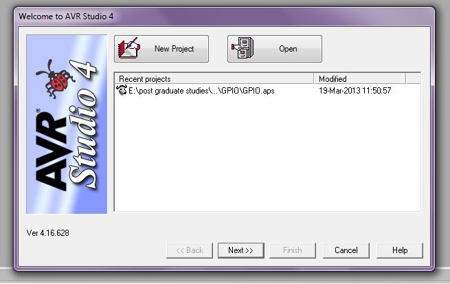
I'll take you in a quick tour how to start your first project From scratch with AVRstudio4
step_1: create a new project
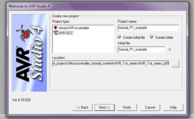
 step_2: choose "AVR GCC" , And Pick-up a name , and Location for your project
 step_3: Select the Target platform you will use "Proteus VSM", and Your Target "ATmega8"
 step_4: window will look like this
 step_5: from Project -> Configuration options Setting the Clock Frequency for your controller
 Let's walk through the Application code:
/****************************************************
* @file tutorial_p1_example.c *
* @Author Islam Essam *
* @date 14 April 2016 *
* @brief AVR Tutorial Series Part I Example *
****************************************************/
/***************************************************
*** Any System Configurations needed ***
***************************************************/
/****************************************************
*** in this part of file we add all INCLUDE files***
****************************************************/
/****************************************************
*** Macros for Local use ****
****************************************************/
/* Function like macros */
/** Any micro could act as a Function to facilitate operations*/
/* Macro Definitions */
/** Common used Values */
#define LOGIC_1 ((unsigned char)1)
/* Application macros*/
/** Every application related common use or user expressed names */
/* Led Blue is connected to PB2 */
#define Led_port PORTB /* Blue Red*/
#define Led_pin 2
/****************************************************
*** Here we shall define Types to be under use ****
*** only by this file ****
****************************************************/
/****************************************************
*** Here we Define any Global Variables needed *****
****************************************************/
/****************************************************
*** Here we Declare Functions (Prototypes) *****
****************************************************/
/** Functions prototypes*/
/****************************************************
*** Here we Define All Functions *****
****************************************************/
int main (void) /* the main Function*/
After we Know the organization of a File, Now it's time to write our application
and here comes the __Main()__ function
here how we should Organize the Main function
int main (void)
{
/* Local Variable definition */
unsigned char SW1_read;
unsigned char SW2_read;
/* Initialization */
/* Define Pins Directions Input/output*/
/* INPUTs */
/* Output */
/* Configurations & Initialization */
/* Perephirals Configurations */
/* Interrupt configurations */
/* System Features Enable / Disable */
/* system wide pull-up should be enabled */
SFIOR &= ( ~(1 << PUD)); // this enables the PULL_UP system wide
/* Global Interrupt enable */
/* WDT */
/* Application code */
/* Apllication Code is the code the system will
be doing Forever, Endless Loop is Needed
So, You should know that your logic will be repeated over and over
and that meet your application NEED
*/
while(1)
{
/* YOUR APPLICATION LOGIC will be written Here */
}//while(1) end
} //main end
Let's Discuss the Application Logic
/* Application code */
/* Apllication Code is the code the system will
be doing Forever, Endless Loop is Needed */
while(1)
{
/* Wait untill the user press any-Key*/
/* Switch 1 & 2 both are off i.e Both are High
SW_1 = 1 && SW_2 = 1
then nothing pressed */
/* Reset Switch Reads for a new Run .. Every time our loop will Start here */
/* our switches are Active low Switches ..
So Values are High when system Start and after finishing every action
to Re-evaluate each time */
SW1_read = ACTIVE_LOW_RESET_VAL ; /* Active Low switches */
SW2_read = ACTIVE_LOW_RESET_VAL ;
/* Chech the software Reads we Re-update every 200ms to see if any switch is pressed */
while ( SW1_read && SW2_read )
{
/* we'll delay the CPU for a while
so as not to keep it 100% Loaded */
_delay_ms(200);
/* update the Switch Read VAR */
/*take a reading from the 2 switches*/
SW1_read = READ_PIN(SW_1_prt,SW_1_pin);
SW2_read = READ_PIN(SW_2_prt,SW_2_pin);
}
/* the loop exit when A key is pressed*/
/* we have 3 use cases
(SW_1) is Pressed Only
(SW_2) is Presses Only
(SW_1 And SW_2) are Pressed Together*/
/* LOGIC
- Check which led
- ON the Led
- wait until condition INvalidated
- OFF the Led
*/
| SW2 | SW1 | state | Logic |
|:------:|:-------:|:----------:|:-------------:|
|0 | 0 | Yellow Led | SW1 ^ SW2 |
|0 | 1 | RED Led | values |
|1 | 0 | Blue Led | values |
|1 | 1 | NONE | Values |
if(! (SW1_read ^ SW2_read )) /* Both are Pressed */
{
/* Both are Pressed */
/* Led_Yellow ON*/
SET_PIN(Led_Yell_prt,Led_Yell_pin);
/* wait untill any butoon is Released
invalidate condition that Led_Yellow is ON */
while ( (LOW_VAL == READ_PIN(SW_1_prt,SW_1_pin))
&& (LOW_VAL = READ_PIN(SW_2_prt,SW_2_pin))
)
{
_delay_ms(200); /* wait ...*/
}
/* Condition INVALIDATED
Led-Yellow OFF */
CLR_PIN(Led_Yell_prt,Led_Yell_pin);
}
else if (! SW1_read)
{
/* Led_Red ON */
SET_PIN(Led_Red_prt,Led_Red_pin);
/* wait untill key released
Or the other Key is pressed */
while ((LOW_VAL== READ_PIN(SW_1_prt,SW_1_pin))
&& ( HIGH_VAL == READ_PIN(SW_2_prt,SW_2_pin))
)
{
_delay_ms(200); /* wait ...*/
}
/* LEd_Red OFF*/
CLR_PIN(Led_Red_prt,Led_Red_pin);
}
else
{
/* Led_Blue ON */
SET_PIN(Led_Blue_prt,Led_Blue_pin);
/* wait untill key released */
while ( (LOW_VAL == READ_PIN(SW_2_prt,SW_2_pin))
&& (HIGH_VAL == READ_PIN(SW_1_prt,SW_1_pin))
)
{
_delay_ms(200); /* wait ...*/
}
/* LEd_Blue OFF*/
CLR_PIN(Led_Blue_prt,Led_Blue_pin);
}
}//while(1) end
##Attachment## AVR_Tut_series_p01_sources.zip contain:
- Acomplete AVRstudio4 project is attached
- proteus simulation is attached for this example as well ##Deliver the way you should## To Code Like Pro You Get to Deliver what you Are Requested to This example could look very simple , but to Meet the Requirements It will Really Bother You :) How to make sure that you meet the Requirements ??
- case1 :
- press SW_1 LED_RED -> ON
- Release SW_1 LED_RED -> OFF
- case2 :
- Press SW_2 LED_BLUE -> ON
- Release SW_2 LED_BLUE -> OFF
- Case3 : Press SW_1 & SW_2 LED_Yellow -> ON
- Release SW_1 LED_Yellow -> OFF & LED_RED -> ON
- Press SW_1 & SW_2 LED_Yellow -> ON & LED_RED -> OFF
- Release SW_2 LED_Yellow -> OFF & LED_RED -> ON
- Release SW_1 & SW_2 -> ALL LEDS Are OFF What we've just did was Writing Testing Plan for your Application :) Start to Test them one by one in order to cover all Cases. You've just made your first concrete step into this World, Feel Thirsty for more ... PART II will get you drink. ##What we will discuss Next ... ###AVR ATmega Tutorial (Series PART II) ... We will Discuss ###
- C API's for GPIO
- Designing a general use Driver for the peripheral, case: GPIO
- Building a Complete system , Integrating the Driver within it
- Real world use case for the Peripheral (mini-project)
- Testing on the Various Levels (Driver / API / Integration)
- ###About me### Find all what you need to know at my Linkedin profile
Comments
BBCode Tags
| BBCode | Rendering |
|---|---|
| [b]bolded text[/b] | bolded text |
| [i]italicized text[/i] | italicized text |
| [u]underlined text[/u] | underlined text |
|
Auto link already enabled. |
http://example.org |
|
Auto image already enabled. |
 |
| [code=php]<?php echo 'Hello!'; ?>[/php] | |
| [quote]quoted text[/quote] | quoted text |
|
[list] [*]Entry 1 [*]Entry 2 [/list] |
|