DIY USB Oscilloscope using a dsPIC
Feb 08, 2017 By Niculescu Vlad
Intro
The main purpose of this article is to create a crude, PC-based oscilloscope. A dsPIC33 is used to take ADC samples of an external signal. The data is sent to a PC via a serial-to-usb converter. The PC runs a custom C# program that displays the waveform. The slope and trigger can be adjusted through the PC app. The PIC microcontroller's ADC can reach a maximum of 1 Million Samples Per Second (MSPS) using 8-bit resolution, which is more than enough for general purpose applications.
Noteable Features
- 1 MSPS ADC performance with external crystal
- Cheap - Entire BOM cost, excluding USB-TTL converter costs < $10.
- Adjustable slope, trigger, and sample rate. GUI Updates every 200ms.
- Input range of 0V-Vdd
- 80% Flash / 20% RAM left for user application (no optimization)
Here is a youtube video showcasing the output on the PC.
Table of Contents
1. Building It
Construction can take a bit of time if you don't purchase the starter kit since you don't have to make a bunch of wires and stick them into the PIM.
1.1 Parts
I used only a few parts. You can optionally just duplicate my digikey order which will auto-fill your cart. Pretty neat.
| Part | Digkey | Description | Purpose |
|---|---|---|---|
| dsPIC33 | MA330020-ND | MODULE PLUG-IN DSPIC33F 44-QFN | Embedded Target |
| 8MHz Crystal | XC1922-ND | CRYSTAL 8.0000MHZ 20PF T/H | Accurate clock for ADC |
| Crystal Capacitors | 399-8916-ND | CAP CER 20PF 50V NP0 RADIAL | Crystal Stabalization |
| Decoupling HF Capacitors | BC2659CT-ND | CAP CER 1000PF 50V X7R RADIAL | Decoupling HF |
| Decoupling LF Capacitors | 493-10470-1-ND | CAP ALUM 4.7UF 20% 16V RADIAL | Decoupling LF |
| USB to TTL converter | 768-1015-ND | CABLE USB EMBD UART 3.3V .1"HDR | PC to MCU Communication |
@note: The USB to Serial converter MUST be TTL levels. There are numerous options out there. I used a custom made converter using the MCP2200 and some level shifters.
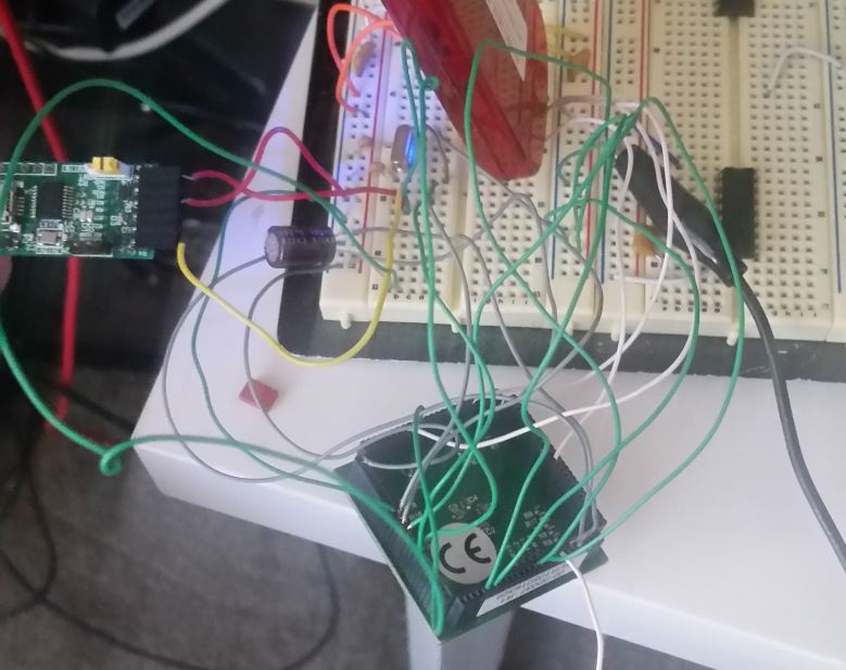
I used a breadboard and multiple small gauge wires to connect to the Plug-in Module (PIM). The typical sized breadboard wires will NOT fit inside the PIM holes! You will need at least 24 gauge or higher. Alternativly, you can just purchase the Explorer 16/32 Board which fits the module without hacking away at the cost of $120. I wanted to do this cheap, so I opted the poor mans route. In hindsight, I should have just purchased the kit since the circuit is extremely fragile.
1.2 Pins
@see this table for more information on the pin connections. The actual part only has 44 pins, however the PIM has 100. Not all of the pins are connected and there is no 1:1 correlation (pin 1 on the PIM != pin 1 on the dsPIC). In addition to the power supply pins from the above document, you will need to connect the following
| Purpose | dsPIC33FJ16GS504 | PIM |
|---|---|---|
| PGC3 - Debugging | 42 | 95 |
| PGD3 - Debugging | 41 | 83 |
| MCLR - Debugging | 32 | 13 |
| Analog Input | 21 | 34 |
| UART RX | 3 | 59 |
| UART TX | 2 | 58 |
| OSC1 - Crystal | 33 | 64 |
| OSC0 - Crystal | 32 | 63 |
In total, you can expect to connect 19 wires into the PIM. This gets kinda crazy.
Connect your PICkit 3 PGD, PGC, GND, MCLR, and VDD to the target. See here for help with your connections. The high-frequency (HF) decoupling capacitors should be placed close to the PIM and power rails. The 4.7uF caps should be placed on the power rail and to VddCORE on the PIM. More general dsPIC33 circuit connection advice here. The TTL-to-USB converter should have its TX be connected to the dsPICs RX. The same logic can be applied for the RX pin. Make sure to connect all of the grounds together. The PICkit 3 can apply 3.3V to Vdd and power the entire circuit.
2 Testing
I used a fancy Agilent function generator to test this project. Whatever input you use must have its GND connected to the dsPIC. Do not use an input signal that is more than Vdd, or rather 3.3V. Doing so may damage the analog input pin. I accidentally damaged one pin by doing this.
- Download the source code attached to this page
- Open it inside of MPLABX. You may need to download the XC16 compiler
- Configure your PICkit 3 to apply 3.3V
- Program, or debug the target
- Connect your input signal into the analog pin (pin 34 on the PIM). Remember to connect the grounds!
- Connect your USB converter into your PC and the TX/RX pins to the dsPIC
- Extract the Visual Studio project from the downloaded zip
- Open it up in Visual Studio Express, which is free
- Compile the project and run it
- Select the correct COM port that corresponds to your TTL converter
- Play around with the trigger to see the analog waveform
I applied a few known waveforms to test the accuracy of the oscope.
2.1 Verify Frequency
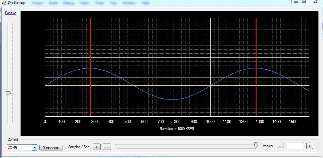
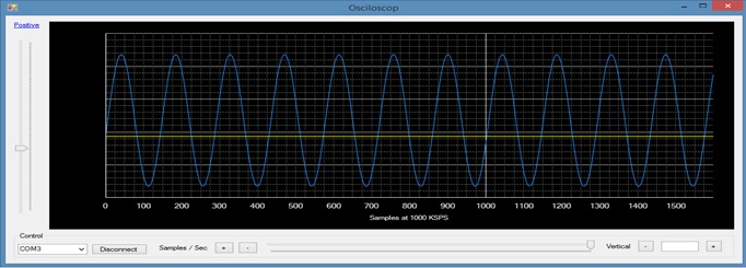
I placed red lines to mark the period. Subtracting 275 from 1275 yields ~1000 samples. Since our PWM is configured to interrupt 1 million times, which triggers an ADC reading, each sample represents 1uS of time. 1000 samples within 1 period marks a 1KHz which matches our function generator.
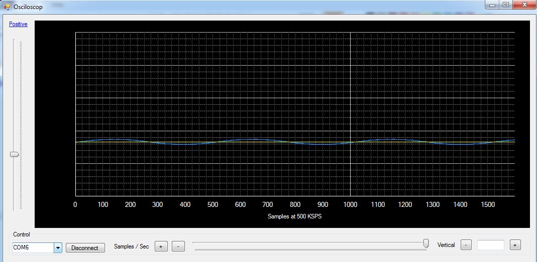
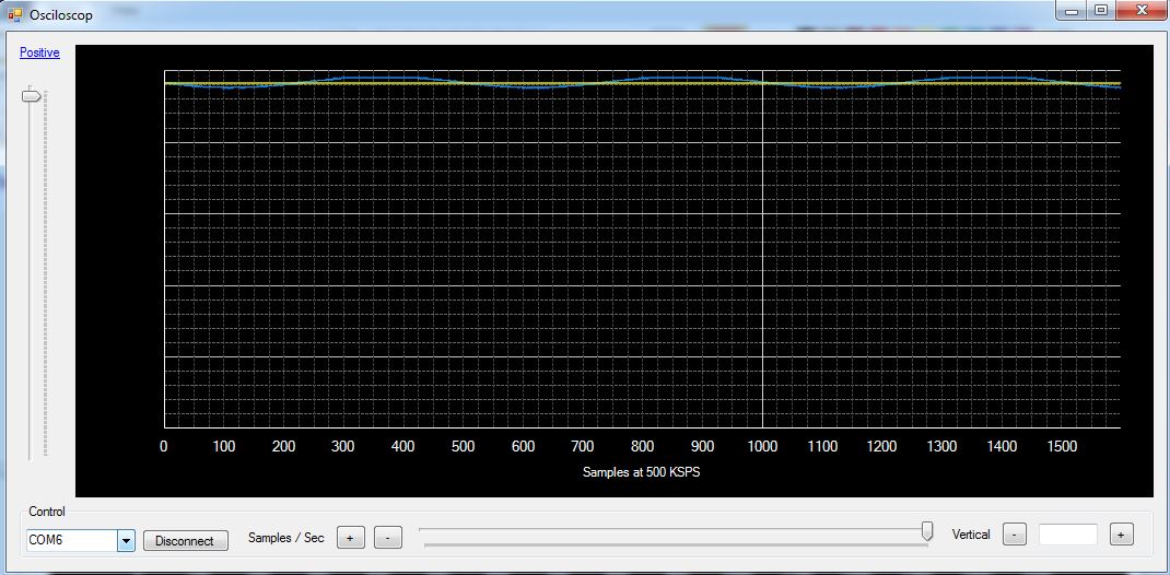
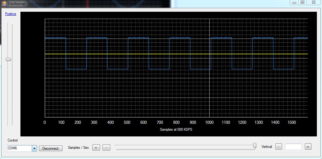
Slowing down the PWM frequency (and hence ADC sampling rate) to 500 KSPS shows a graph like this
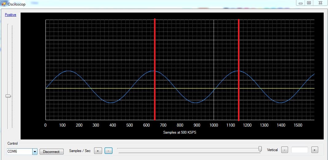
(1150-650) = 500 samples * (1s/500000 ksps) = 1ms => 1/1ms = 1KHz. As you can see, changing the sample rate will change the waveform on the scope, but the *measured signal is still the same just like in a real scope.
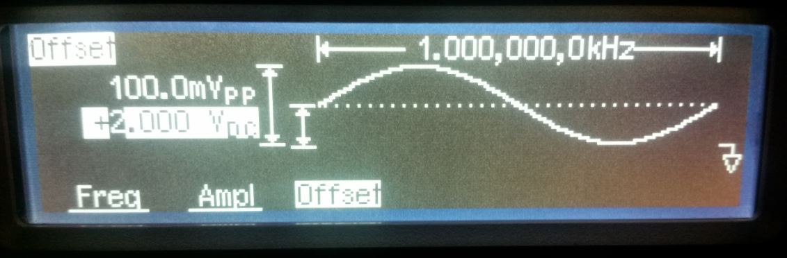
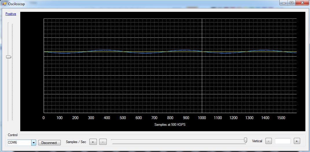
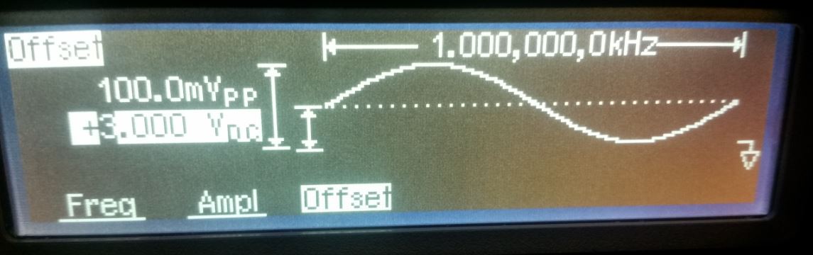
2.2 Verify Voltage
The Y-Axis corresponds to the voltage. The absolute bottom should represent 0V and the top should equal the ADC reference voltage of around 3.3V minus some slight overhead.
1Vdc offset with 100mV ripple
2Vdc offset with 100mV ripple
3Vdc offset with 100mV ripple
As you can see by the yellow horizontal line, the voltages are within where we expect them to be on the scope.
Can you guess the frequency, Vdc offset, and Vpp (peak-to-peak) from the following graph?
Answer: 2KHz, 1Vpp, 2Vdc offset.
2.3 Verify Trigger
This is self-explanatory. Move the trigger away from the expected plot to see the GUI stop updating the waveform and vice versa
2.4 Verify Slope
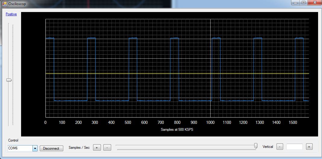
The slope direction is calculated by taking two readings and subtracting the newest from the oldest and checking if the subtraction yields a positive or negative number. A positive triggered signal should appear as follows. Notice how this pulse train is first triggered on the sharp RISING edge.
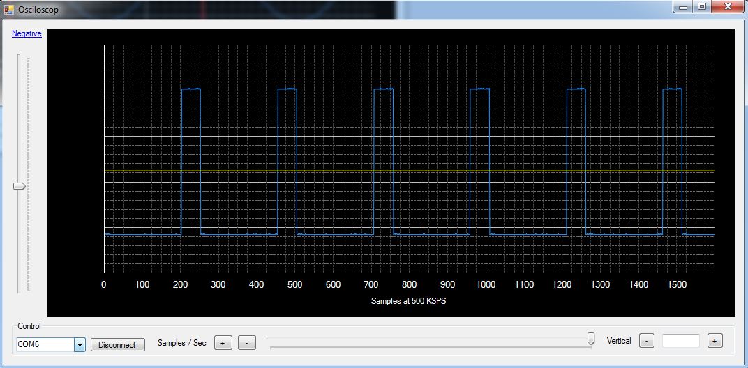
Notice how the NEGATIVE edge is now detected when the GUI switches to negative edge detection
3 Firmware
Most of the code is written in C with the exception of the ADC routine which had to be in assembler. Most of it is simply initialization.
The PC initiates all conversions. The microcontroller will sample for a new package when requested by the PC. The USB buffer and MCU buffers will not be at risk of being overflowed in this model. When the confirmation command is received, the microcontroller enters the Receiving Interrupt (UART Rx Interrupt), and starts processing the small data payload received from PC. This payload contains information regarding slope, trigger level, and sampling speed and is processed using a non-blocking function in order to keep the ADC interrupt functioning at a fixed rate.

I will highlight the most important code snippets below. The rest of the code such as port initialization can be seen in the attache firmware and its mostly self explanatory
3.1 State Machine
The program is built on the model of a state-machine, respecting the basic principle that the system can be found just in one state at a certain moment on time. The states are: OFF_STATE, TON_STATE, ON_STATE, TOFF_STATE, and WAIT_STATE. The OFF_STATE initializes the microcontroller. TON_STATE enables the interrupts and prepares for going to ON_STATE, which is the main loop. Here the device checks if the 1600 points were sampled in order to create the package to send up to the PC. The system goes in TOFF_STATE and subsequently WAIT_STATE if a fault occurs such as a memory overflow. This is where interrupts are disabled and faults are checked.
The sampling loop is initiated once the PC payload is parsed. The enable bit in the PWM signal is set with a period dictated by the sampling speed communicated by the PC. The PWM signal generates an interrupt which puts the micro in its PRETRIG state. Every ADC value is compared to the trigger level. The micro also checks the slope of the signal by interpreting the difference between two consecutive values. If the difference is positive, then the slope is positive. Otherwise it is a negative slope. The sampling occurs until the 1600 length array is full.
3.1 ADC
Because a high sampling rate is required, I couldn't make the sampling inside of a loop, like a for or while. The dsPIC33FJ16GS504 instead has a unique feature in which it can generate an internal high frequency trigger derived from a fast PWM signal. This interrupt causes the ADC to initiate a conversion. The sampling rate of the PIC depends on the PWM period and its sample and hold timing. The A/D is implemented on the dsPIC as a SAR.
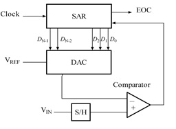
The convertor has a DAC, a successive approximation register, and a comparator. The register provides the digital code for DAC, which generates values of voltage until it finds out the most appropriate value which is most near to the input signal. The comparator compares the DAC's output to the input and feeds the 'yes/no' result back into the SAR for processing. The precision of the approximation depends on the A/D converter's resolution, which is 10 bit for this PIC. Most embedded microcontrollers have an 8 or 10 bit ADC.
3.2 Sampling Algorithm
The entire state machine had to be written in assembly due to the speed requirements. A sampling rate of 1MSPS results in just (40 MHz/1 MHz) = 40 instructions per sample. You can look at the dsPIC30 Family Reference Manual for more information regarding execution speed. As a side note, the midrange and enhanced mid-range PIC devices execute 4 times slower than the dsPIC30 family (Fosc/4). MPLAB's compiler would translate the above mentioned states in more than 40 assembly instructions which would make the reconstructed signal inaccurate.
A fast sample rate coupled with high ADC resolution is ideal to recreate the analog signal as closely as possible. The amount of memory to save the samples however becomes troublesome on a low-end microcontroller. This dsPIC has a limited amount of memory - just 2KB.
The accuracy of the conversion was lessened in lieu of space. The sampled resolution was lessened from 10 bits to 8 bits in order to conserve additional memory. If the controller has 2KB of RAM, and a sample is 1 byte wide, this means that a total of 2048 samples will fill the entire memory. The actual program will limit the sample buffer to 1600 bytes in order to reserve some space for the rest of the program. The ADC samples are collected into a buffer and it operates as a FIFO buffer.
Waiting for the trigger level is a very fast process so this part is implemented in assembler. This checks to ensure if the slope is + or - and that the trigger level is observed before taking an ADC sample.
__ADCP0Interrupt:
	PUSH.S
	BTG	LATA,#3		     ;  bit toggle
	MOV	ADCBUF0, w1	     ;  load value from ADC in w1
	BTSC	_Status, #STATUS_TRIG_BIT    ;  if set, go in TRIG state
                                             ; else skip next instruction when pretrig ends
	BRA	TRIG
	BTSC	_Status, #STATUS_PRETRIG_BIT	; if in pretrig
	BRA	PRETRIG                         ;still waiting for the trigger level
                                                ; else if trigger stopped
	BRA	ENDADCISR

PRETRIG:
	MOV	_TriggerValue, w0	; load trigger value to wreg
	BTSC	_Status, #STATUS_SLOPE_BIT	; skip if 0 – according to slope
	BRA	NEGSLOPE                ; the slope bit was set by user

 POSSLOPE:
	CP	ADCBUF0			; CP- compares with value in w0
	BRA 	LT, ENDADCISR
	CP	_OldValue		; Compare with Old value to
                                                ; verify the slope
	BRA	GT, ENDADCISR           ; if condition not met, go out from interrupt
	MOV	_XVal, w0
	MOV	w0, PTPER
	BCLR	_Status, #STATUS_PRETRIG_BIT     ; clear bits when going in the next state
	BSET	_Status, #STATUS_TRIG_BIT
	BRA	TRIG                     ; branch in the trig state

 NEGSLOPE:
	CP	ADCBUF0			 ; ADCBUF0-TrigValue
	BRA 	GT, ENDADCISR
	CP	_OldValue		 ; OldVal-TrigVal
	BRA	LT, ENDADCISR            ; the same as previous case, but slope condition is opposed
	MOV	_XVal, w0
	MOV	w0, PTPER
	BCLR	_Status, #STATUS_PRETRIG_BIT
	BSET	_Status, #STATUS_TRIG_BIT
	BRA		TRIG
Here, the samples are stored. Note that we are using a pointer to a global variable vi that holds the ADC samples. You cannot pass variables into an assembler program like you would in a typical C program which is why the variables are declared global.
TRIG:
	LSR   w1, #2, w2	;  right shift by 2 the ADC
	MOV   _viaddress, w0	;  load the current index to w0
	MOV.B	w2, [w0]	;  put in v[w0]
	INC   _viaddress	;  increment pointer address
	INC   _vi		; increment actual vi, so to compare to  max
	MOV   #1600, w0		;  max is 1600
	CP    _vi		; 14 compare vi-w0
	BRA   NZ, ENDADCISR	;  jump to 1f if not zero

	                         ; sampling complete

	MOV   #MHZ_CAL_VALUE, w0
	MOV   w0, PTPER
	BSET  _Status, #STATUS_DATAREADY_BIT
	BCLR  _Status, #STATUS_TRIG_BIT
	CLR   _vi			; reset
	MOV   #_v, w0			; we put in viaddress the address of v[0]
	MOV   w0, _viaddress

ENDADCISR:                              ; with this, the interrupt is left
	MOV 	w1, _OldValue
	BCLR	IFS6,#ADCP0IF		; Clear ADCP0 interrupt flag
	POP.S
RETFIE
3.3 Communication
The data is sent to the PC at 57000 baud as soon as the buffer is full. The package has the following ASCII form: snp10[arrays contain]end. This is sent over a single USB endpoint. snp and end are used as delimiters in the parsing process. A DataReady and TransmissionInProgress flags were added to aid in synchronizing the micro with the PC.
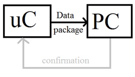
The PIC receives an interrupt anytime a byte is received from the PC. It quickly saves it into a small buffer and awaits for a special command sequence before taking samples. Data is sent to the PC by simply polling the TXREADY bit before sending the next byte.
A new acquisition process starts when a new command is received. This command also includes the adjustments in a small buffer. Very important: The sampling process has to start from the same value of signal (and also the same slope). This value can be adjusted by the user and is called the TRIGGER LEVEL.
Below shows the parsing of the data packet sent from the PC
    //the adjustments information is extracted from the array
    YVal = RXBuffer[RXBuffI - 4]; //amplification coefficient – unused, because //there isn't any input circuit
    XVal = RXBuffer[RXBuffI - 5]; //timebase = sampling rate
    XVal = MHZ_CAL_VALUE << XVal;
    TriggerValue = (RXBuffer[RXBuffI - 6] << 2); //value of the trigger level
    if(RXBuffer[RXBuffI - 7] == '0')    //the slope bit
    	Status.bits.Slope = SLOPE_POSITIVE;
    else
    	Status.bits.Slope = SLOPE_NEGATIVE;
    RXBuffI = 0; //the index is reset to 0 and the first state is left

    if( (Status.bits.Trig == 0) && (Status.bits.DataReady == 0) )
    	Status.bits.PreTrig = 1; //the package is completely received
The entire buffer will now be shifted out the UART TX register, byte by byte. Note the numerous special characters that are used to synchronize between the PC and dsPIC.
void Comm_Process_Data(void)
{
if(Status.bits.TxInProgress == 0) //if other transmission is not in progress, start it
{
if(Status.bits.DataReady == 1) //if data is ready to be sent
{
TXBuf_Counter = 0; //prepare the transmission, by initializing the index
Command_Id = 0xA0;
Status.bits.TxInProgress = 1; //make the transmission flag 1
}
}
if( (Status.bits.TxInProgress == 1) && (U1STAbits.TRMT) ) //if transmitting and uart-//transmitter is free
{
if(TXBuf_Counter < 4)
{
switch(TXBuf_Counter) //notify the PC to start listening to samples
//by sending “snp†– start new packet
{
case 0: U1TXREG = 's'; break;
case 1: U1TXREG = 'n'; break;
case 2: U1TXREG = 'p'; break;
case 3: U1TXREG = Command_Id; break;
}
}
else
{
switch(Command_Id)
{
case 0xA0: //report arrays with all data
if(TXBuf_Counter < 1604)
U1TXREG = v[TXBuf_Counter-4]; //send a new sample
else
switch(TXBuf_Counter) //prepare to end transmission
{
case 1604: U1TXREG = 'e'; break;
case 1605: U1TXREG = 'n'; break;
case 1606:
U1TXREG = 'd';
Status.bits.TxInProgress = 0;
Status.bits.DataReady = 0;
break;
};
break;
};
}
//has transmitted a character, now increment
TXBuf_Counter++;
}
}
4. GUI:
C# was chosen because it's easy to use, fast, and has the support of .NET's libraries. Simply choose the virtual COM port that is connected to the PIC and the program should function as an oscilloscope. The interface provides adjustments for trigger level and for time-basis, using for each of two a track-bar. A toggle button sets the slope and it's also included a button for setting sampling speed.
There are three timers that manage different functionalities.
-
SerialTimerchecks every 200ms if a new package is available and starts processing it. This includes updating the graph. -
SnapshotTimerchecks the communication and sends a confirmation package to the micro (with the adjustments also), giving it a flag to resend a new data pack -
InterfaceTimerupdates the GUI anytime the number of samples is changed.
The structure of the sent data pack is presented below, with a smaller size than received pack.
snp[slope bit][trigger value][time base]yend
5. Improvements
- Can configure the ADC in differential mode to allow a greater range of analog inputs. Adding a front-end to the ADC pin would also allow negative voltages.
- It would be pretty cool to build an enclosure around the hardware. Matter of fact, creating a PCB from the schematic would be a good start.
Comments
BBCode Tags
| BBCode | Rendering |
|---|---|
| [b]bolded text[/b] | bolded text |
| [i]italicized text[/i] | italicized text |
| [u]underlined text[/u] | underlined text |
|
Auto link already enabled. |
http://example.org |
|
Auto image already enabled. |
 |
| [code=php]<?php echo 'Hello!'; ?>[/php] | |
| [quote]quoted text[/quote] | quoted text |
|
[list] [*]Entry 1 [*]Entry 2 [/list] |
|